MiniMIPS is a compact and efficient RISC (Reduced Instruction Set Computer) processor inspired by the MIPS architecture.
This project was developed as part of the Computer Organisation and Architecture Lab [CS39001] course.
It provides a step-by-step workflow for:
✔️ Designing in Verilog
✔️ Simulating in Vivado
✔️ Deploying on FPGA
MiniMIPS implements a simplified ISA (Instruction Set Architecture) with a modular design philosophy.
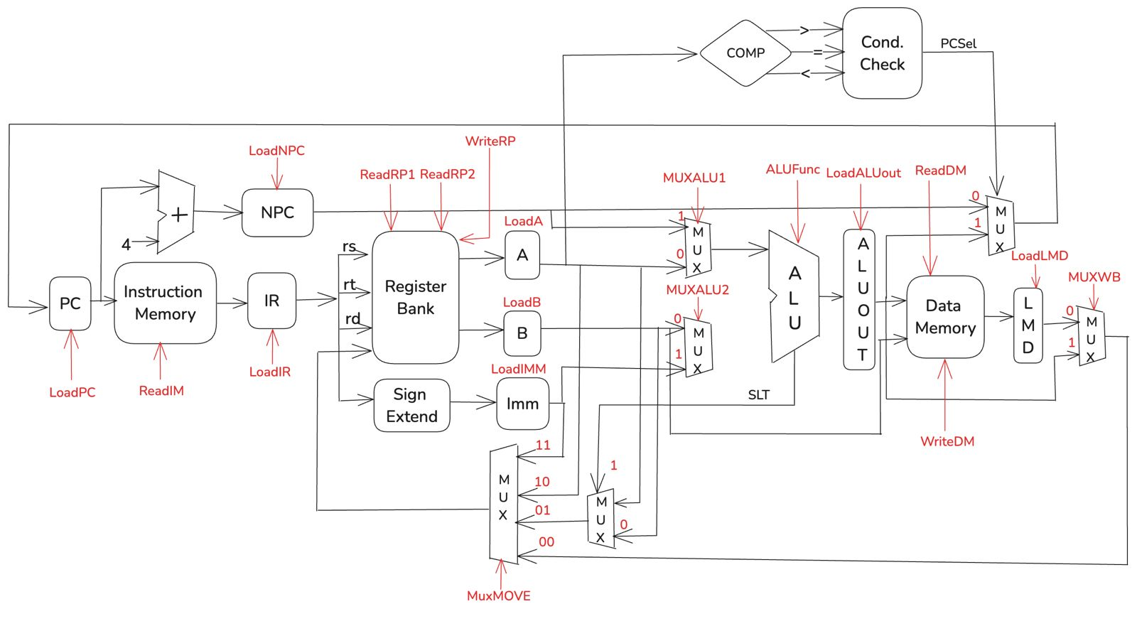
It consists of a datapath, control unit, and memory modules, all integrated into a top-level processor that can be deployed on an FPGA.
The datapath structure of MiniMIPS:
- Open Vivado → create project → add Block Memory Generator (BRAM).
- Configure Instruction Memory & Data Memory.
- Add wrappers:
BRAM_Data.vandBRAM_Instructions.v.
- Copy all modules from
DataPath/. - Verify interfaces, check signal connectivity, and run testbenches.
- Import
Control Unit&Branch Control. - Validate opcode decoding and branch logic.
- Add
Processor.v→ connect datapath & control. - Set as Top Module.
- Run initial synthesis.
- Reference:
instruction.s. - Follow ISA format, comment instructions, and validate against ISA doc.
python3 assembler.py <input_file.s>- Produces
.coefor memory initialization.
- Assign
.coefiles to BRAMs in Vivado. - Re-run synthesis.
- Add testbench for
Processor.v. - Verify control signals, ALU operations, memory access.
- Add
FPGA_Wrapper.v. - Map processor I/O to FPGA pins.
- Define pins in
FPGA_XDC.xdc.
- Run Synthesis → Implementation → Bitstream generation.
- Connect board via USB/JTAG.
- Upload
.bitusing Vivado.
- Input select pins → view ALU output or register bank.
- Debug incorrect outputs by rechecking signals & control logic.
| Folder / File | Description |
|---|---|
DataPath/ |
Verilog modules for datapath |
ControlPath/ |
Verilog control unit modules |
Memory/ |
BRAM configurations |
Processor.v |
Top-level integration |
FPGA_Wrapper.v |
FPGA wrapper |
FPGA_XDC.xdc |
FPGA pin constraints |
assembler.py |
Assembly → .coe converter |
- Xilinx Vivado (tested on 2020.2+)
- FPGA Board (e.g., Xilinx Artix-7 / Basys-3)
- Python 3.8+ (for assembler)
- Clone repo:
git clone https://github.com/<your-username>/<your-repo>.git
- Open Vivado → Import all Verilog files.
- Run steps from Setup Process.
- Program FPGA → test assembly code execution.
Pull requests are welcome!
For major changes, open an issue first to discuss your ideas.
This project is licensed under the MIT License – see the LICENSE file for details.