
This Project is done by Eng. Abduallah Damash, and assigned to me by Assoc. Prof. Dr. Tayfun Nesimoğlu as part of EE312 (DIGITAL ELECTRONICS) course.
If you have any issues or comments on the project, contact me on Linkedin (https://www.linkedin.com/in/engabduallah). I also provided all the files that I used in this project so that you can try it by yourself.
This project will build upon the designing of standard CMOS inverter to design more complex digital CMOS combinational and sequential building blocks:
A. An enabled ring oscillator circuit design and analysis, which will be utilized to extract a Delay Correlation Factor and Input Capacitance for reference inverter propagation delayestimates in a given 2μm technology node, using simple analytical models.
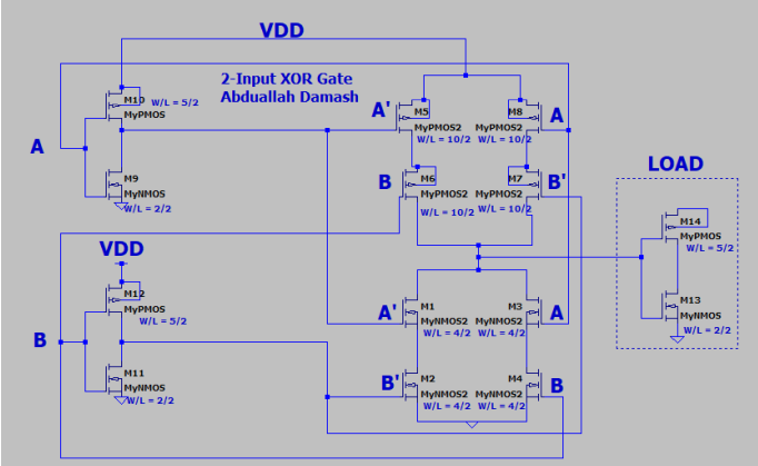
B. 2-input XOR gate design using standard CMOS design technology, to achieve balanced LH and HL propagation delay performance.
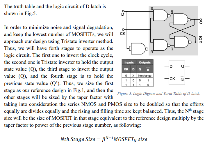
C. D-type latch design.
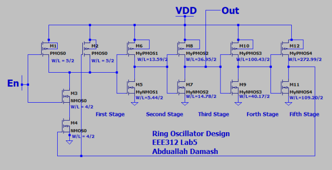
Ring Oscillator Designing:
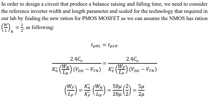
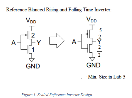
as seen in Fig.1. Then, we need to size the first stage which is the NAND gate using worst path methodology. After that, since the rest stages are cascade inverter, we need to use the optimal value of taper factor as 𝛽𝑂𝑡𝑚 ≈ 𝑒 and scale the other stage accordingly so that the propagation delay remains balanced. Also, for low-cost consideration, the design will consider the lowest number of MOSFET and try to minimize the utilization area by using the optimal value of taper factor.
2-input XOR Gate Design:
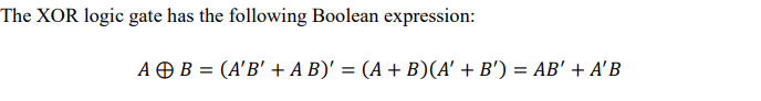
The expression for the XOR gate is what we will use to build the pull-down network, and the second expression is used to build the pull up network. The third expression is the simplified expression for the XOR operation.
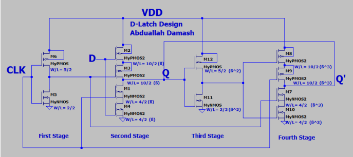
D-type Latch Design:
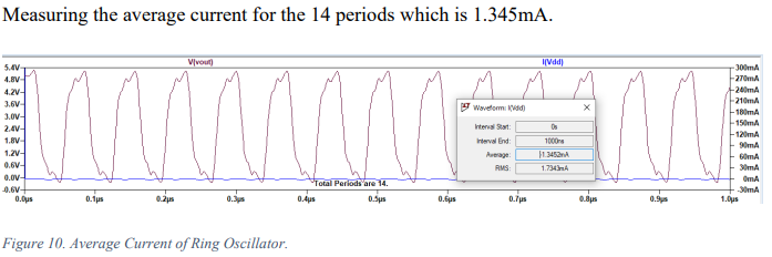
Ring Oscillator Simulation:
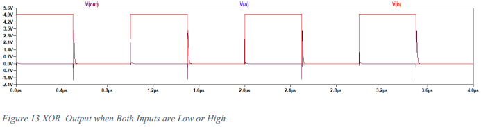
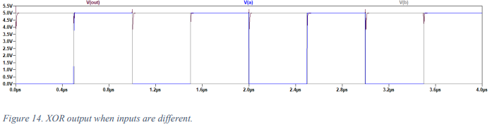
2-Input XOR Gate Simulation:
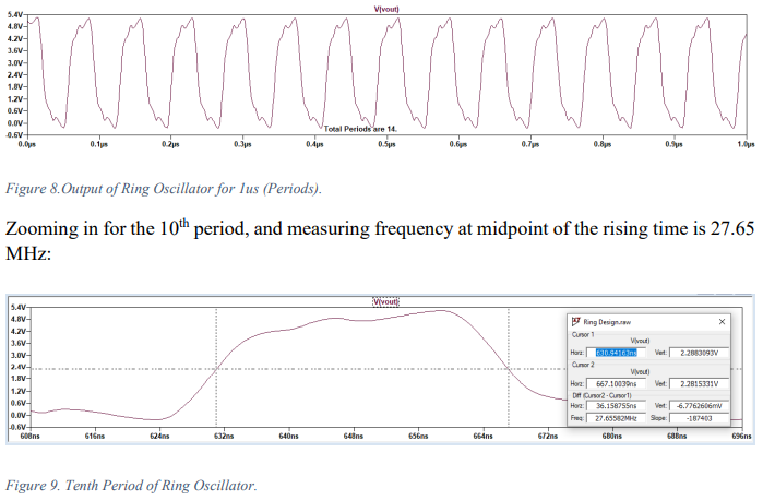
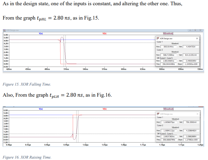
Measurement of Worst-Case Rising Time and Falling Time:
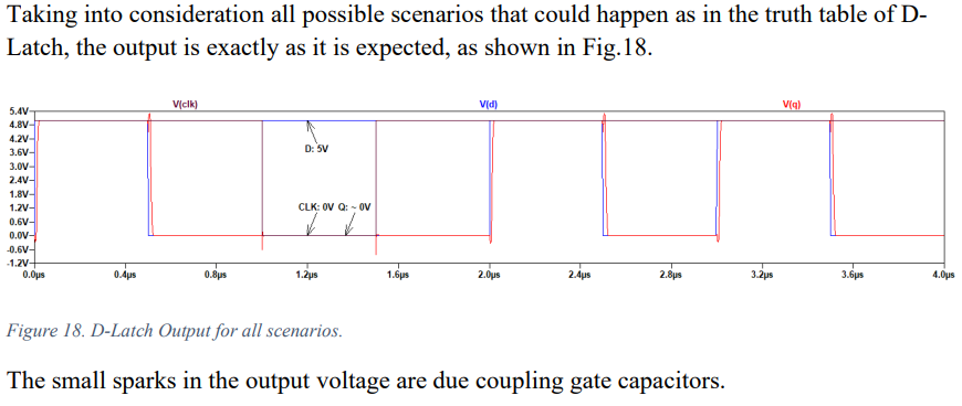
D-Type Latch Simulation:
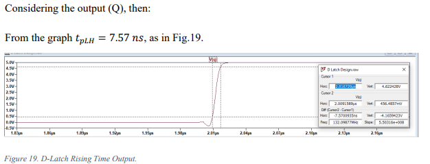
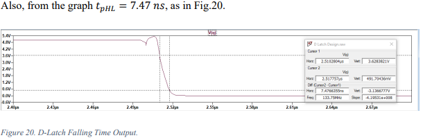
Measurement of Propagation Delays:
Enjoy it.
All rights saved, if you want to use any piece of the code, mentioning my name will be enough.